

Products
Atomic layer deposition system
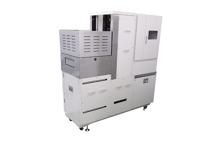
AFALD-8
A capacitive-coupling-type plasma source is installed, enabling the deposition of high-quality thin films at low temperatures. A wide range of materials can be deposited by using gases of various materials for ALD.
- Superior Step Coverage
- Precise Thickness Control
- Pinhole-free
- Low Damage
ALD method is a thin film deposition method realizing superior step coverage and film-thickness controllability. Even in the structure having high aspect ratio or complex 3D configuration, it is possible to form thin films controlled at the atomic level. In addition to the conventional benefit of ALD, AFALD ensures the deposition of high-density and high-quality films by enhancing the reactivity using a plasma precisely controlled in milliseconds order. This system can accommodate max. four metal precursors and max. three reactive gases, and by combining it with a proper transfer module, all your needs from R&D to massproduction can be met.
- Product Features
- Standard specification
- ALD Principle
Standard mounted CCP plasma source
- Controllable in milliseconds for low-damage
- stable deposition.
Wide range of option selection
- Transfer system can be selected from manual loader to cluster module type loader.
- The number of material vaporizers and reactive gases are selectable.
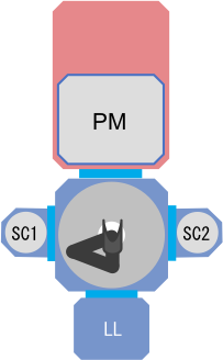
| Item | Full Cluster Type | Compact Cluster Type | Load-lock Type |
|---|---|---|---|
| Configuration | 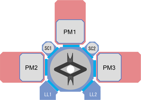 |
 |
 |
| Process Modules | Max. 3 | 1 | 1 |
| Transfer Robot | W Arm | Single Arm | Linear Actuator (Auto/Manual) |
| Load-Locks | Max. 2 | 1 | 1 |
| Sub Chambers | Max. 2 | Max. 2 | None |
Software that is powerful and easy to operate
- Interface enabling the intuitive operation
- Configuration function which can be set arbitrarily
- Standard installed abundant log functions.
Easy maintenance by well-designed Inner-Chamber.
Designed for lower material cost
A unique patented vaporizer having excellent material consumption efficiency by controlling the feeding pressure is adopted.
| Item | Specification |
|---|---|
| Maximum substrate size | φ200 mm |
| System dimensions (W×D×H) | 600 × 1700 × 2060 mm |
| System weight | Approx. 700kg |
| Reactor type | Plasma, Thermal |
| Plasma generation method | CCP 13.56MHz Max.1000W |
| Number of metal precursors | Max. 4 |
| Number of reactive gases | Max. 3 (Mass flow controller) |
| Maximum substrate temperature | 400℃ (Set value) |
| Vacuum pump | Dry Pump (Suitable for chemicals) |
| Hot wall | Standard feature |
| Piping heating | Standard feature (Individually controllable) |
| Pressure control | Auto Pressure Control valve (APC) (Pressure in each room can be controlled individually.) |
| Process gas trap | Standard feature |
| User interface | PC/AT (Personal computer) |
| Module controller | PLC |
| Utilities | |
| Electrical supply | 3-phase 200VAC 50/60Hz 150A |
| P-N2 | 0.3~0.6MPa 10SLM |
| P-O2 | 0.3~0.6MPa 6SLM |
| N2 | 0.3~0.6MPa 65SLM |
| Compressed air | 0.5~0.7MPa 15SLM |
| Cooling water | 0.1~0.3MPa 5L/min 0.5MPa 5L/min |
ALD Principle
ALD (Atomic Layer Deposition)
ALD (Atomic Layer Deposition) proposed by T.Suntola, Finland in 1974.
ALD Reaction Model: Deposit film AB by alternate supply of reactant Ax and By
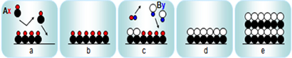
Dep.Oxide Film
- a) Supply Precursor: Reaction between reactant Ax and Substate (Self-Limited)
- b) Purge: Purge excessive Ax by inert gas
- c) Supply Oxidant: Reaction of oxidant By with Ax.
- d) Purge: Purge excessive By and by-product xy.
Superior Step Coverage
By the self-limiting function of surface reaction on a wafer, AFALD ensures superior step coverage.
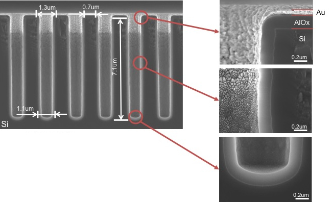 ▲ Cross-sectional SEM image
※Au film on ALD-Al2O3 thin-film surface
▲ Cross-sectional SEM image
※Au film on ALD-Al2O3 thin-film surface
Thickness can be controlled at the atomic level by the number of ALD cycles.
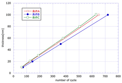 ▲ Relation Between the Number of ALD Cycles and Film Thickness
※Data obtained on MPAD-40s
▲ Relation Between the Number of ALD Cycles and Film Thickness
※Data obtained on MPAD-40s
Excellent electrical properties
By using plasma enhancement, high break down voltage and low leak current property can be achieved even at lower temperature
Superior water vapor barrier property
In comparison with CVD, etc., a thinner film can achieve the equivalent water vapor barrier property.
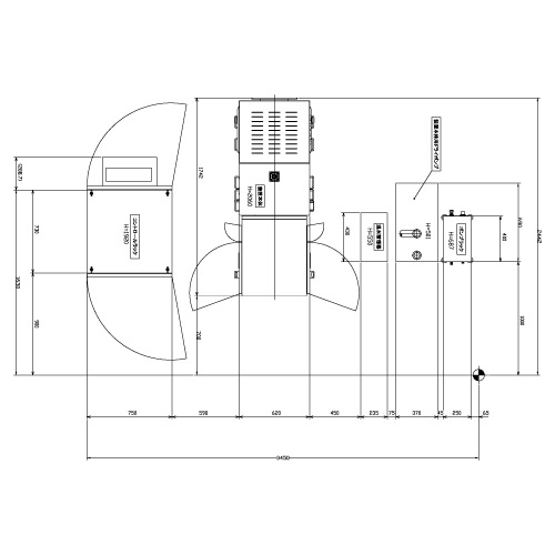
Drawing & Diagram

Contact Us
TEL 045-787-7203 / FAX 045-787-8472
Please feel free to contact us, you can reach us with phone or thru contact form here.
